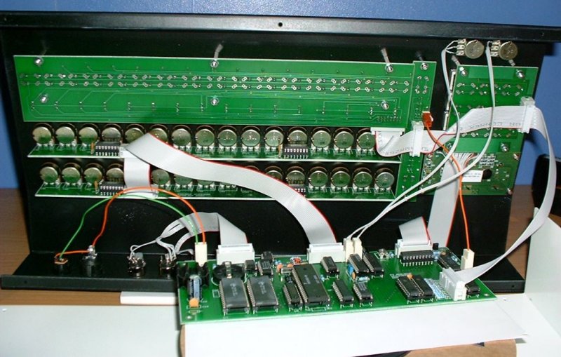
| DIN output board | ||
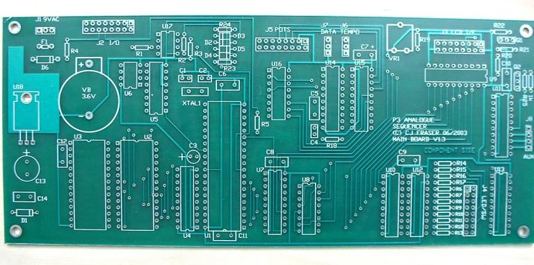
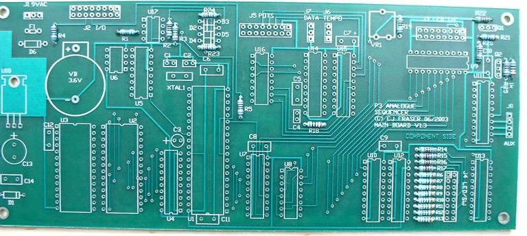
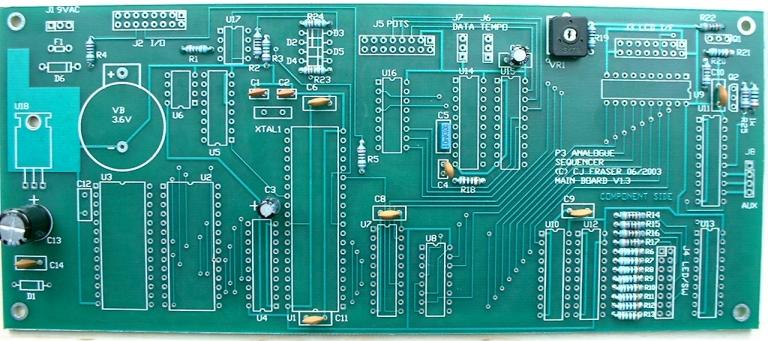
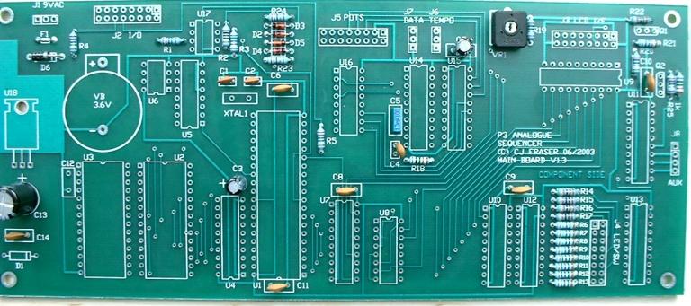
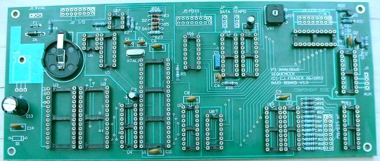
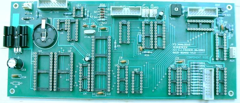
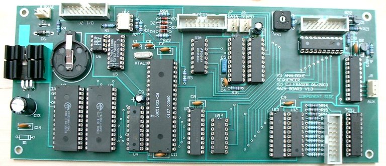
| Main board | (schematic) | |
| Function switch / LED board | (schematic) | |
| Step Switch / LED board | (schematic) | |
| Keypad board | (schematic) | |
| Upper pot board | (schematic) | |
| Lower pot board |
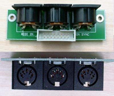
| Gnd | 1 | 2 | DIN SYNC PIN 3 |
| Gnd | 3 | 4 | DIN SYNC PIN 1 |
| Gnd | 5 | 6 | n/c |
| Gnd | 7 | 8 | n/c |
| Gnd | 9 | 10 | MIDI OUT PIN 5 |
| Gnd | 11 | 12 | MIDI OUT PIN 4 |
| Gnd | 13 | 14 | MIDI IN PIN 4 |
| Gnd | 15 | 16 | MIDI IN PIN 5 |